ASMPT combines high-speed chip assembly directly from wafers with SMT placement in a single machine
As automotive applications, 5G and 6G, smart devices and many other devices require ever more compact and powerful components, advanced packaging becomes one of the key technologies. With its new SIPLACE CA hybrid placement solution, market and technology leader ASMPT combines semiconductor and SMT production in a single machine and integrates the production of SiPs (system-in-packages) directly into the SMT line. The SIPLACE CA2 processes SMDs and dies taken directly from the wafer in a single step at speeds of up to 50,000 dies or 76,000 SMDs per hour with a precision of up to 10 μm @ 3 σ. The result: maximum flexibility, efficiency, productivity and quality paired with enormous savings in terms of time, cost, space and tape waste. In addition, the advantages of SIPLACE technology are now also available to the semiconductor world with “full single die level traceability” and the various automation options made possible by ASMPT’s flexible and manufacturer-independent Open Automation concept for the integrated smart factory.
In high-speed SiP manufacturing, such as for smartphones and tablets, some dies are processed directly from the sawn wafer while others are flip chips and components such as passive components from tape & reel. Until now, this is usually done in two separate processes. With the new highly flexible and powerful SIPLACE CA2 placement platform, ASMPT is integrating the ability to process dies directly from the sawn wafer into the high-speed SMT line.
“The SIPLACE CA2 brings together what belongs together in the SiP age and opens up new dimensions in advanced packaging. The highly flexible configuration and leaner processes create new opportunities, open up new markets and customer groups for electronics manufacturers, and increase productivity while reducing costs, thus delivering significant competitive advantages,” explains Sylvester Demmel, Senior Product Manager at ASMPT SMT Solutions.
Die buffer and parallelization solve speed problems
One of the main obstacles to the combined handling of SMT components and dies used to be the slow process of fetching dies directly from the wafer. On the wafer, which is delivered sawed, the dies are affixed to a carrier film from which they must first be detached before they can be assembled – a process that is almost impossible to accelerate.
The SIPLACE CA2 solves this problem with a buffer storage module that operates similarly to a placement head and can hold 16 new dies (plus four on the flip unit) while the placement head itself is placing dies. This separates the pickups from the wafer from the die placement and parallelizes them, thus bringing the machine’s placement performance close to that of the SMT world. In this way, the innovative solution processes up to 40,000 flip-chips or up to 50,000 chips in the die-attach process, or up to 75,000 SMT components from tapes per hour with a placement accuracy of up to 10 μm @ 3 σ.
Maximum flexibility for die processing
Unrivaled, the SIPLACE CA2 has a wafer exchange system that holds up to 50 different wafers. A wafer swap takes only 6.5 seconds. This saves valuable space on the shop floor, creating room for more fast machines and automated storage and transport solutions.
Cost-saving and sustainable
Collecting the dies directly from the wafer also makes the die-taping process unnecessary. Eliminating tapes offers several benefits. Depending on the production volume, the cost savings can run into the millions – for the taping material itself as well as for its storage and disposal. In addition, taking the chips directly from the wafer makes the production more sustainable because it avoids tape waste that can be huge.
Full traceability and software integration
The full traceability of components that are already mandatory in many markets continues to pose major challenges in the world of semiconductors. The SIPLACE technology offers great benefits in this field with its “full single die level traceability”, which automatically logs each die’s pick-up position as well as its placement position on the board.
In addition, the SIPLACE software offers fast program and product changeovers, placement program portability to any machine of the same type, and fast and comprehensive substrate mapping. Many applications in the efficiency- and productivity-enhancing WORKS shop floor management suite are also available for the SIPLACE CA2 for things like setup verification, optimization, and logistics.
Open interfaces for the integrated smart factory
In addition to the SECS/GEM interface, which is important for semiconductor production, the SIPLACE CA2 offers the IPC-CFX open communication standard – one of the basic prerequisites for the integrated smart factory. As a result, seamless data communication can now be ensured also for the die handling process – on the shop floor as well as with factory and enterprise solutions. In this way, the SIPLACE CA2 can be fully integrated into Open Automation, the modular, manufacturer-independent and ROI-based automation concept of ASMPT.

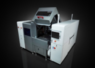
The SIPLACE CA2 boosts productivity in advanced packaging by combining classic SMT with die-attach and flip-chip assembly.

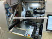
Interior view of the SIPLACE CA2: The placement machine can simultaneously process classic 8-millimeter tapes as well as dies directly from the wafer.

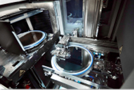
A sawed wafer gets fed from the wafer exchange unit into the multi-wafer system. The wafer swap takes only 6.5 seconds.

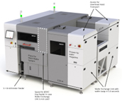
The SIPLACE CA2 delivers maximum performance and flexibility in a footprint of only 2.56 × 2.50 meters
